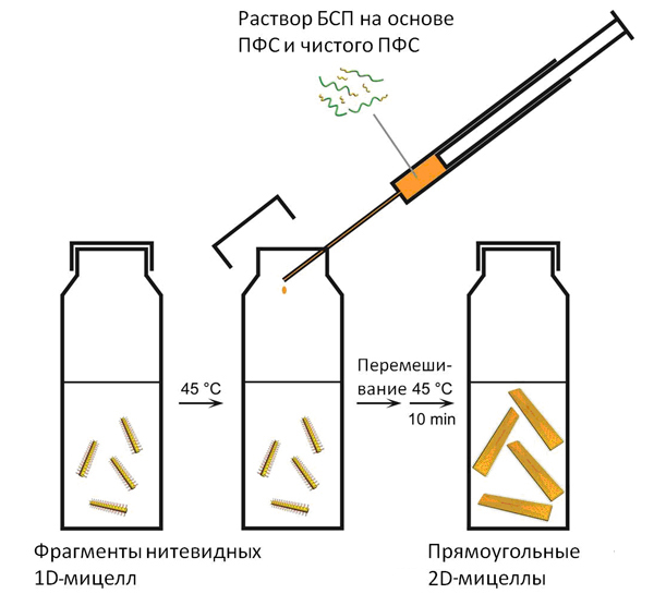
Fig. 1. Scheme for obtaining rectangular 20nm thick micelles with controlled surface area. The structure obtained by adding the block copolymer (BSS) with short polukristallichnoy part (poliferrotsenilsilan, PPS) mixed with short to pure PPS Cylindrical micelles based on SFC.
British and Canadian chemists first succeeded in self-assembly method to obtain two-dimensional rectangular nanostructures with full control over the area and the chemical composition of the surface. Success was achieved through the use of block copolymers with semicrystalline block, finding the correct ratio units of length and added to the free chains of semi-crystalline polymer solution. This technology can be useful in the future for use in fluorescence imaging, nanoelectronics, catalysis, liquid kristallax, moving nano- and mikromashinax or therapeutic media.
At the end of the XX century, it became clear that the nano-sized particles (measuring 1-100 nm in at least one dimension) have properties that do not appear in the macrocosm. This happens because with a decrease in particle size to nanoscale it becomes a significant contribution to the properties of the surface properties of the object. Another reason for the change of properties is the fact that at the nanoscale appear laws of quantum mechanics. Thus, it appears that these two-dimensional structures capable of exhibiting remarkable electronic properties, qualitatively different from all first observed in 2004 when a group of physicists led by Andrew Geim and Konstantin Novoselov first graphene samples were obtained. Today, hundreds of experimental groups investigate the electronic properties of graphene.
Classify nanoparticles easiest on the degree of reduction of dimension: two-dimensional – the quantum plane, one-dimensional – quantum wires, zero-dimensional – quantum dots. The whole range of reduced dimensions conveniently explained by the example of carbon nanoparticles (Fig. 2).

Figure 2. Carbon nanoparticles. From left to right: zero-dimensional fullerene, carbon nanotube one-dimensional, two-dimensional graphene.
The world of nanotechnology, of course, is not limited to carbon: almost any nanoscale material in their own unusual and potentially interesting. How did they receive? For zero-dimensional nanomaterials (quantum dots) are suitable, generally known chemical methods, because the quantum dot – this is usually a large molecule. For one- and two-dimensional materials needed new approaches. It should be noted that the dimensions, in which no nano material (where its dimension greater than 100 nm), there is a theoretical possibility to alternate the composition of the surface and thus get more interesting materials for various applications. However, modifying graphene and other similar materials are very difficult to chemically. Creating a two-dimensional nanostructures with controlled dimensions and chemical composition of the surface – one of the unsolved problems of nanotechnology. With the discovery of graphene, this area of research received a major boost, but, apart from a few examples, the problem has remained unsolved to this day.
Self-assembly of macromolecules in solution – the most elegant, convenient and economical method of producing nanomaterials, and that this method is theoretically possible to create structures with controlled surface composition if alternate macromolecules, which are added to the solution.
A team of scientists from the University of Bristol (UK) and the University of Toronto (Canada), inspired by his recent success in the control of one-dimensional nanostructures achieved using the self-assembly of block copolymers (BSP), in which one of the blocks was a semi-crystalline poliferrotsenilsilan (PPS), I tried to use a similar approach for two-dimensional nanostructures.
Recall that BSP – a polymer in which the two parts (two blocks) or consist of different monomers. Self-assembly of block copolymers in solution is due to different solubility of the two parts. Polukristallichnost – is the ability of the polymer to crystallize, that is orderly shape. The prefix “semi” is needed here because the folding of polymer in the crystal are always nekristallichestkie (amorphous) fragments.
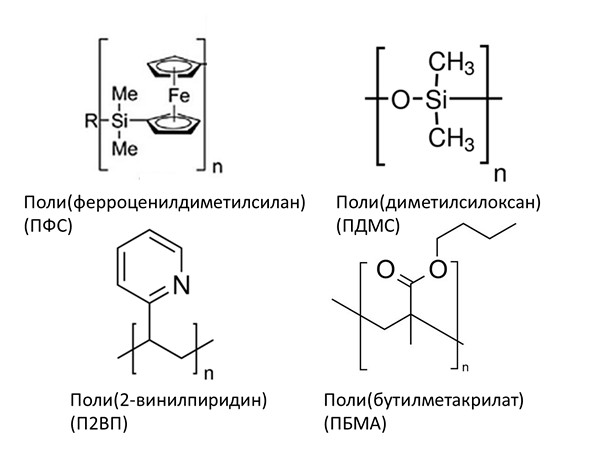
Figure 3. The polymers mentioned in the text, in order of their appearance. Numerical index n of the polymer name means the degree of polymerization – the average number of monomer units in the polymer molecule. Nitrogen on a pyridine ring P2VP capable of binding to metals and some other molecules – a property that has been used by the authors (see below in the text.)
The success of a one-dimensional structure was due to the fact that the semi-crystalline part of the block copolymer was much shorter than the soluble part. When self-assembly of soluble long chain of BSP on the surface of the micelles formed, interfering with each other, are not allowed to create a flat structure, and gets the thread. When shortening the chain soluble micelles in BSP or not obtained at all, or precipitated.
Then we decided to experiment with self-assembled BSP mixture of long-soluble part and a pure poliferrotsenilsilana (PPS). The idea was that the additional chain PPS, PPS sokristallizuyas a unit in the copolymer is to create additional surface area, allowing the soluble chains do not interfere with each other. The mixture is added to a solution of short threadlike micelles, so that they serve as a center of crystallization.
After several unsuccessful attempts to experiment with mixtures PFS28-PDMS560 / PFS20 and PFS38-P2VP502 / PFS20 hit the mark (Fig. 4). Addition polymers with short micellar solution resulted in a rectangular structure height ~ 20 nm, and their size (area) is fully controlled by the quantity of added polymer. Since micelles edges are not closed, it is possible to add further block copolymer, and it will not adhere to the remainder micelle.
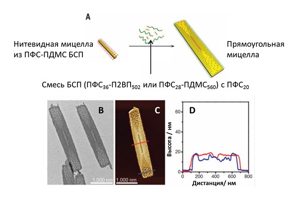
Fig. 4. A – a schematic representation of the micelles producing rectangular mixture BSS / PPS in a ratio of 1: 1 by weight. B – picture rectangular micelles obtained by a transmission electron microscope (TEM). C – a picture obtained by atomno-silovogo mikroskopa (AFM). D – the height of the structure, izmerennaya AFM. It matches the color of the curve lines in Fig. 4, C – at this point the height was measured. Drawing from discussion article in Science
To demonstrate the control of the area and the chemical composition of the surface, the authors raised the micelle, sequentially adding to the initial rectangular micelle-P2VP PPS polymers with different color (fluorescent) groups (Fig. 5).

Fig. 5. Coloured rectangular micelles by self-assembly prepared by sequentially adding PPS PDMS molecules with fluorescent dyes attached. Top row – a schematic representation; middle row – images with a confocal microscope; bottom row – the pictures of individual micelles, made with the help of a structured Illumination Microscopy (see Structured illumination microscopy.).
Thus, the authors demonstrated the possibility to alternate the chemical composition of the micelle surface. How to use this opportunity? One of the polymers in the composition of the micelles used in the self-assembly – P2VP – coordinative bond capable of binding to metals. By adding platinum nanoparticles with a diameter of 2 nm to a solution of micelles, alternating on the surface of PDMS and P2VP authors selectively tied P2VP chain, without affecting the PDMS. In other words, in a region with a surface turned crosslinked P2VP platinum nanoparticles.
After adding tetrahydrofuran (THF), which dissolves all normal conditions of PPS-containing block copolymers, the authors only PPS dissolved PDMS. After dissolving turned nanoramki – rectangular cross-linked micelles of P2VP with a hole in the center. The holes can be produced of any size, depending on the size and P2VP PDMS blocks (Fig. 6). In micelles with a widest aperture thickness of the side walls of <100 nm – this is actually a hybrid of a cyclic one-dimensional and two-dimensional nanomaterial.
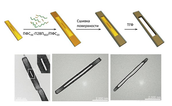
Fig. 6. Getting nanoramok. The primary structure consists of PPS-PDMS. On it built up layer-P2VP PPS, who later selectively cross-linked platinum nanoparticles. Dissolution uncrosslinked central portion in tetrahydrofuran (THF) gives nanoramku. Above – a schematic of the process image. Below – nanoramok shots with different values of the holes made by a transmission electron microscope (TEM).
Having mastered the technique, the authors have done many more experiments to demonstrate its power:
Micelles were prepared from eight alternating blocks of PPS and PPS-PDMS P2VP (Fig. 7, A), and the units can be rotated endlessly.
Made as a micelle of the three chemically different blocks of the SFC-PDMS-P2VP PPS and PPS-PBMA (Fig. 7, B), and to do nothing to prevent them from four or five different blocks, and so. D.
Micelles were treated PPS and PPS-PDMS-P2VP nanoparticles of silica (average diameter 70 nm).
The silica particles are fragments of SiOH, that form hydrogen bonds with a P2VP pyridines. Fig. 7 C shows that nanoparticles (black dots) are selectively attached to the block with P2VP micelles.
Prepared readily soluble micelles are longer than 60 m and a width greater than 20 microns without significant defects (Fig. 7, D), wherein the size of the area is not limited solubility.
Finally, the authors showed that their structures are strong enough to manipulate them using optical tweezers (Fig. 7, F), blagdarya so they can be put on the surface in a predetermined order. Fig. 7, the E illustrates how micelles with a green rim posted on the university name abbreviation, in which they learned to do: UOB – University of Bristol.

Fig. 7. A – a snapshot of the micelles of the eight alternating blocks of PPS and PPS-PDMS P2VP. B – picture micelles of three different blocks (in the order from the center: PPS-PBMA, PFS-PDMS-P2VP PPS). C – a snapshot of the micelle-PDMS PPS and PPS-P2VP treated silica nanoparticles (70 nm) adhered selectively to P2VP through hydrogen bonds. D – long shot micelles more than 60 microns and a width of 20 m, made using atomno-silovogo mikroskopa (AFM). E – snapshot micelles lined using optical tweezers in the form of abbreviations UOB (top); a picture of the same place taken by confocal microscope (bottom). F – sxematicheckoe manipulation micelles image using optical tweezers. Pictures A, B, C and E (top) made by a transmission electron microscope (TEM).
The authors – chemists and materials scientists – do not put in the work to find the problem and demonstrate the unique physical properties of the new structures. They believe that this technology will continue to be interested in physics and started a revolution. Since today known PFC-containing block copolymers with a huge number of chemical modifications in the soluble portion can be obtained nanostructure having on the surface of anything: from biomolecules to semiconductors to metals a good half of the periodic table to complex molecular architectures. The authors note that mozhet technology in the future is suitable for use in fluorescence imaging, nanoelectronics, catalysis, in liquid kristallax, moving nano- and mikromashinax or therapeutic nositelyax. Designated a lot of imagination.
Source: Huibin Qiu, Yang Gao, Charlotte E. Boott, Oliver E. C. Gould, Robert L. Harniman, Mervyn J. Miles, Stephen E. D. Webb, Mitchell A. Winnik, Ian Manners. Uniform patchy and hollow rectangular platelet micelles from crystallizable polymer blends // Science. 2016. V. 352. I. 6286. P. 697-701.